Lateral MoS2 p-n junction formed by chemical doping for
- Classification:Chemical Auxiliary Agent
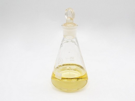
- CAS No.:117-84-0
- Other Names:DOP Bis(2-ethylhexyl) phthalate
- MF:C24H38O4, C24H38O4
- EINECS No.:201-557-4
- Purity:99.0%Min
- Type:Plasticizer, Dioctyl Phthalate
- Usage:PVC Products, Coating Auxiliary Agents, Leather Auxiliary Agents,
- MOQ:200kgs
- Package:200kgs/battle
- Certificate::COA
This study suggests an effective way to form a lateral p-n junction by the h-BN hard masking technique and to improve the photoresponse of MoS2 by the chemical doping
Thus, this study suggests an effective way to form a lateral p n junction by the h-BN hard masking technique and to improve the photoresponse of MoS 2 by the chemical doping process.
Ultimate thin vertical p–n junction composed of two Nature
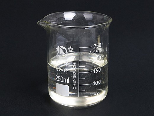
- Classification:Chemical Auxiliary Agent, Chemical Auxiliary Agent
- cas no 117-84-0
- Other Names:Dop
- MF:C6H4(COOC8H17)2
- EINECS No.:201-557-4
- Purity:99.5%min
- Type:Adsorbent, plasticizer
- Usage:Plastic Auxiliary Agents, Plasticizer
- MOQ::10 Tons
- Package:25kg/drum
- Shape:Powder
- Payment:T/T
- Application:PVC Plasticizer
Choi, M. S. et al. Lateral MoS2 p-n junction formed by chemical doping for use in high-performance optoelectronics. ACS Nano 8,9332–9340 (2014) . Article CAS Google Scholar
Lateral MoS 2 p-n Junction Formed by Chemical Doping for Use in High-Performance Optoelectronics Min Sup Choi 1, 2, Deshun Qu 1, 2, D curves of MoS 2 p-n diodes before
Lateral MoS2 p-n junction formed by chemical doping for
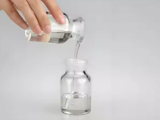
- Classification:Chemical Auxiliary Agent
- CAS No.:117-84-0
- Other Names:DOP/Dioctyl Phthalate
- MF:C6H4(COOC8H17)2
- EINECS No.:201-557-4
- Purity:99.5%, 99.9%min.
- Type:Oil drilling
- Usage:Coating Auxiliary Agents, Leather Auxiliary Agents, Plastic Auxiliary Agents, Rubber Auxiliary Agents
- MOQ:200kgs
- Package:200kgs/battle
- Volume Resistivity:114
This paper demonstrates a technique to form a lateral homogeneous 2D MoS2 p-n junction by partially stacking 2D h-BN as a mask to p-dope MoS2. The fabricated lateral MoS2
Choi, M. S. et al. Lateral MoS 2 p–n junction formed by chemical doping for use in high-performance optoelectronics. ACS Nano 8,9332–9340 (2014). Article CAS PubMed
Lateral MoS2 p-n Junction Formed by Chemical
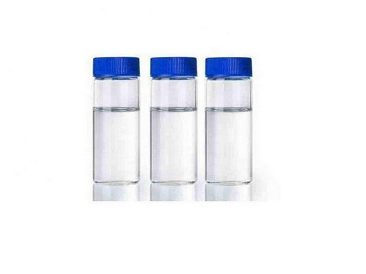
- Classification:Chemical Auxiliary Agent
- CAS No.:117-84-0
- Other Names:DOP
- MF:C24H38O4, C24H38O4
- EINECS No.:201-557-4
- Purity:99%min
- Type:pvc additive
- Usage:Plastic Auxiliary Agents, Plastic Auxiliary Agents, Rubber Auxiliary Agents
- MOQ::10 Tons
- Package:25kg/drum
- Advantage:Stable
- Payment:T/T
Thus, this study suggests an effective way to form a lateral p-n junction by the h-BN hard masking technique and to improve the photoresponse of MoS2 by chemical doping process. Fabrication of the
The lateral MoS2/MoO3 p-n junction exhibits a highly efficient photoresponse and ideal rectifying behavior, with a maximum external quantum efficiency of ∼650%, ∼3.6 mA
Lateral monolayer MoS2 homojunction devices prepared by
- Classification:Chemical Auxiliary Agent, Chemical Auxiliary Agent
- cas no 117-84-0
- Other Names:Dioctyl Phthalate DOP
- MF:C6H4(COOC8H17)2
- EINECS No.:201-557-4
- Purity:99.5%, 99.9%min.
- Type:Chemical additives, Chemical dop plasticizer 99%
- Usage:Coating Auxiliary Agents, Leather Auxiliary Agents, Paper Chemicals, Plastic Auxiliary Agents, Rubber Auxiliary Agents
- MOQ:200kgs
- Package:200kgs/battle
- Place of Origin::China
- Advantage:Stable
After the doping of N 2 +, the work function increased and the Fermi level of the p-type monolayer MoS 2 shifted towards the valance band and a built-in electric field from the n
Here, we employ benzyl viologen (BV) as an effective electron dopant to part of the area of a (p-type) few-layer BP flake and achieve an ambient stable, in-plane P–N junction. Chemical doping with BV molecules modulates the electron density and allows acquiring a large built-in potential in this in-plane BP P–N junction, which is crucial
- How efficient is a lateral Mos 2 p n junction?
- The fabricated lateral MoS 2 p–n junction with asymmetric electrodes of Pd and Cr/Au displayed a highly efficient photoresponse (maximum external quantum efficiency of ∼7000%, specific detectivity of ∼5 × 10 10 Jones, and light switching ratio of ∼10 3) and ideal rectifying behavior.
- How are lateral monolayer MOS homojunctions prepared?
- In this article, the lateral monolayer MoS homojunctions were prepared by a nitrogen plasma selective doping technique. The monolayer MoS thin films were synthesized by chemical vapor deposition and characterized by photoluminescence, atom force microscope and Raman spectroscopy.
- What is the voltage of Mos 2 p n junction?
- In solar cell applications, the vertical MoS 2 p–n junction showed a short-circuit current (ISC) of 5.1 nA and an open-circuit voltage (VOC) of 0.6 V. The current and voltage obtained at the maximum output power (Imax and Vmax) were 2.2 nA and 0.3 V, respectively.
- What are atomic force microscopic images for a MoS2?
- Atomic force microscopic images (scale bars are 3 µm) for a MoS2(a) before and (b) after 20 mM AuCl3doping. The formation of Au nano-aggregates comprises the surface charge transfer between AuCl4 -ions and MoS 2. 3 2. Electrodes and chemical doping effects for MoS2transistor
- How does ambipolar carrier transport differ from unipolar MoS2 p n junctions?
- Unlike usual unipolar MoS2, the MoS2 p–n junctions show ambipolar carrier transport, current rectification via modulation of potential barrier in films thicker than 8 nm and reversed current rectification via tunnelling in films thinner than 8 nm.
- Does degenerate doping with NB affect MoS2 crystals?
- However, substitutional doping in two-dimensional semiconductors is at a comparatively early stage, and the resultant effects are less explored. In this work, we report unusual effects of degenerate doping with Nb on structural, electronic and optical characteristics of MoS2 crystals.