Semiconductor Doping: Definition, Types,
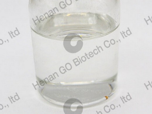
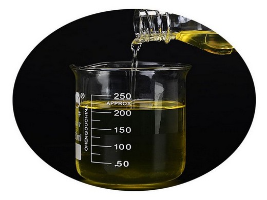
- Classification:Chemical Auxiliary Agent
- CAS No.:117-84-0
- Other Names:Dioctyl Phthalate DOP
- MF:C6H4(COOC8H17)2
- EINECS No.:201-557-4
- Purity:99
- Type:Plasticizer Colorless Oily Liquid DOP for pvc and rubber
- Usage:Coating Auxiliary Agents, Electronics Chemicals, Leather Auxiliary Agents, Plastic Auxiliary Agents, Rubber Auxiliary Agents
- MOQ:200kgs
- Package:200kgs/battle
- Application:PVC Plasticizer
There are two main types of semiconductor doping: P-type and N-type. Together, they give rise to an extrinsic semiconductor. 1. P-type. In P-type doping, impurities create an excess of positively charged holes in the crystal
Chemical doping is an important approach to manipulating charge-carrier concentration and transport in organic semiconductors (OSCs)1–3 and ultimately enhances
OpINg Of sIlICON Neutron Transmutation Doping of AT
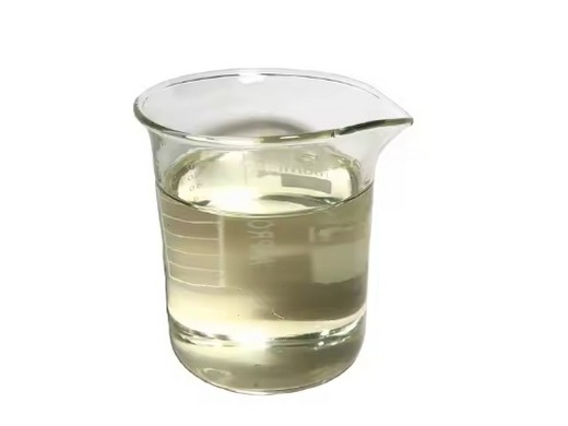
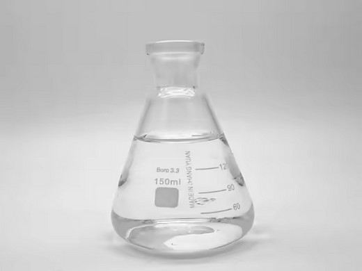
- Classification:Chemical Auxiliary Agent
- CAS No.:117-84-0
- Other Names:DOP, diocty phthalate, 1,2-phthalate
- MF:C24H38O4
- EINECS No.:201-557-4
- Purity:99.5, ≥99.5
- Type:Adsorbent, Carbon Black
- Usage:Coating Auxiliary Agents, Plastic Auxiliary Agents, Rubber Auxiliary Agents
- MOQ::10 Tons
- Package:25kg/drum
- Shape:Powder
- Application:PVC Plasticizer
. p. ; 30 cm. (IAEA-TECDOC series, ISSN 1011-4289 ; no. 1681) ISBN
The chemical doping of molecular semiconductors is based on electron-transfer reactions between the semiconductor and dopant molecules; here, the redox potential of the
Doping in 2D Nature Electronics
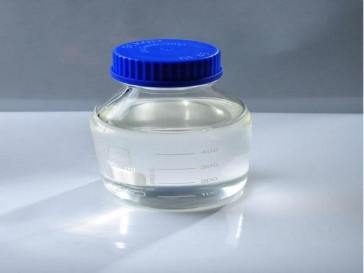
- Classification:Chemical Auxiliary Agent
- CAS No.:117-84-0
- Other Names:DOP Bis(2-ethylhexyl) phthalate
- MF:C6H4(COOC8H17)2
- EINECS No.:201-557-4
- Purity:99 %
- Type:Plasticizer, Dioctyl Phthalate
- Usage:Coating Auxiliary Agents, Electronics Chemicals, Leather Auxiliary Agents, Plastic Auxiliary Agents, Rubber Auxiliary Agents
- MOQ:200kgs
- Package:200kgs/battle
- Advantage:Stable
- Payment:T/T
In comparison, molybdenum disulfide field-effect transistors that have been directly doped with the same molecular dopant (triphenylphosphine, an n-type dopant) exhibit a
Efficient doping for charge-carrier creation is key in semiconductor technology. For silicon, efficient doping by shallow impurities was already demonstrated in 1949 ().In the development of further semiconductor
7.1.4: Semiconductors- Band Gaps, Colors,
- Classification:Chemical Auxiliary Agent, Chemical Auxiliary Agent
- cas no 117-84-0
- Other Names:Dioctyl Phthalate
- MF:C24H38O4
- EINECS No.:201-557-4
- Purity:99.5
- Type:Chemical additives, Chemical dop plasticizer 99%
- Usage:PVC Products, Coating Auxiliary Agents, Leather Auxiliary Agents,
- MOQ:200kgs
- Package:200kgs/battle
- Application:PVC Plasticizer
The Fermi level of a doped semiconductor is a few tens of mV below the conduction band (n-type) or above the valence band (p-type). As noted above, the doping of semiconductors dramatically changes their conductivity. For
“Doping” of semiconductors—that is, the local manipulation of their conductivity—is a key technology for electronic devices. Without doping, for example, a gallium nitride sample larger than the White House would be
Doped Semiconductor Nanomaterials: Applications
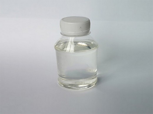
- Classification:Chemical Auxiliary Agent
- CAS No.:117-84-0
- Other Names:Dop
- MF:C6H4(COOC8H17)2
- EINECS No.:201-557-4
- Purity:99
- Type:Plasticizer, Dioctyl Phthalate
- Usage:Coating Auxiliary Agents, Leather Auxiliary Agents, Paper Chemicals, Plastic Auxiliary Agents, Rubber Auxiliary Agents
- MOQ::10 Tons
- Package:25kg/drum
- Shape:Powder
- Place of Origin::China
- Item:T/T,L/C
Doping of Semiconductor Nanomaterials. It is well-known that most semiconductors are ceramic materials with a defined crystalline structure; when an atom or a
“Doping” of semiconductors—that is, the local manipulation of their conductivity—is a key technology for electronic devices. Without doping, for example, a gallium nitride sample larger than the White House would be
- What is chemical doping of molecular semiconductors?
- Provided by the Springer Nature SharedIt content-sharing initiative The chemical doping of molecular semiconductors is based on electron-transfer reactions between the semiconductor and dopant molecules; here, the redox potential of the dopant is key to control the Fermi level of the semiconductor1,2.
- What is semiconductor doping?
- Semiconductor doping is a key process in electronics. It involves adding tiny amounts of specific impurities to a pure semiconductor material, like silicon, to change its electrical properties. This process helps the semiconductor conduct electricity better and makes electronic devices like transistors and diodes work properly.
- What is chemical doping?
- Provided by the Springer Nature SharedIt content-sharing initiative Chemical doping is an important approach to manipulating charge-carrier concentration and transport in organic semiconductors (OSCs)1–3 and ultimately enhances device performance4–7.
- What are the most successful products based on doping?
- The most successful product so far is the organic light-emitting diode display with a multibillion U.S. dollar market, which are using doping by controlled coevaporation of small-molecule semiconductors and dopant molecules ( 5 ). The microscopy nature of doping in organic semiconductors is strongly different from inorganic semiconductors ( 6 ).
- Is silicon a doped material?
- Silicon is instrumental as a matrix material to be doped in a majority of semiconductor devices, while other materials, although at lesser extent, are used as well. An intrinsic semiconductor , also called an undoped semiconductor, is a pure material without any significant dopant species present.
- How does doping work at the heterostructure interface?
- Efficient doping at the heterostructure interface is achieved by charge transfer from the wide bandgap semiconductor to the narrow bandgap semiconductor. The main advantage of this doping technique is the avoidance of ionized impurity scattering in the undoped narrow bandgap semiconductor.